Saturday, December 5, 2015

Maxwell Mesh method Solved problem with Examples

Definition

This method involves a set of independent loop current assigned to as many Maxwell mesh meshes as it exist in the circuit and these currents are employed in connection with appropriate resistances when the KVL equation are written.

Circuit theory Example :


circuit example Maxwell Mesh method
 Using KVL :
  • For the loop A : E1 - IA.(R1+R3) - I3.R3 = 0
  • For the loop B : E2 - IB.(R2+R3) - IA.R3 = 0
Note: mesh currents IA and IB are evaluated by simultaneous substitutions of the equations formulated from each loop or mesh using KVL.

I1 = |IA|     I2 = |IB|     I2 = |IA + IB|

Solved problem :

Solve this circuit for V using Maxwell's mesh method.
Solved problem

  • 4.0 V
  • 5.2 V
  • 2.6 V
  • 3.5 V

Solution and circuit analysis:

Re-draw the circuit:
mesh analysis solved problems

Apply KVL on the loop 'dabcd'

(IA - IB)2 - IB(8) - (IB + IC)2 = 0
Note : IA = 6A ; IC = 3A

Substitute:
(6 - IB).2 - 8.IB - (IB + 3).2 =0
12 - 2.IB - 8IB - IB - 6 = 0
IB = 0.5 A

V = IB(8) = 0.5 x 8
V = 4 Volts

Friday, December 4, 2015

Solved Problems on Series-Parallel resistive circuits with Example

Introduction

Very rarely are we lucky enough to run across straight forward series or parallel circuits. In general, all electronic equipment is eomposed of many components that are interconnected to form a combination of series and parallel circuits. In this lesson, we will be combining our knowledge of the series and parallel.

The Christie Bridge Circuit

Who invented the Wheatstone bridge circuit? It was obviousiy Sir Charles Wheatstone. Or was it?
The Wheatstone bridge was actuaily invented by S.H. Christie of the Royal Military Academy at Woolwich, England. He described the circuit in detail in the Philosophical Transactions paper dated February 28,1833. Christie’s name, however, was unknown and his invention was ignored.
Ten years later, Sir Charles Wheatstone called attention to Christie’s circuit. Sir Charles was very well known, and from that point on, and even to this day, the circuit is known as a Wheatstone bridge. Later, Werner Siemens would modify Christie’s circuit and invent the variable-résistance arm bridge circuit, which would also be called a Wheatstone bridge.
No one has given full credit to the real inventors of these bridge circuits, until now!

Christie bridge

Series Parallel circuits Solved problems

Figure 5-1 (a) through (0 shows six examples of series-parallel resistive circuits. The most important point to learn is how to distinguish between the resistors that are connected in series and the resistors that are connected in parallel, which will take a little practice.
One thing that you may not have noticed when examining Figure 5-1 is that:
Circuit 5-1(a) is equivalent to 5-1 (b)
Circuit 5-1 (c) is equivalent to 5-1 (d)
Circuit 5-1(e) is equivalent to 5-1 (f)
When analyzing these series-parallel circuits, always remember that current flow de-termines whether the resistor is connected in series or parallel. Begin at the negative side of the battery and apply these two rules:
  1. If the total current has only one path to follow through a component, that component is connected in series.
  2. If the total current has two or more paths to follow through two or more components, those components are connected in parallel.
  3. Referring again to Figure 5-1, you can see that series or parallel resistor networks are easier to identify in parts (a), (c), and (e) than in parts (b), (d), and (f). Redrawing the circuit so that the components are arranged from left to right or from top to bottom is your first line of attack in your quest to identify series- and parallel-connected components..
Electronic Series parallel circuits simple

Problem 1:

Refer to Figure 5-2 and identify which resistors are connected in series and which are in parallel.

Schematics Series Parallel Circuit
5-2 Series-parallel circuit exemple

Answers of Problem 1:

First, let’s redraw the circuit so that the components are aligned either from left to right as shown in Figure 5-3(a), or from top to bottom as shown in Figure 5-3(b). Placing your pencil at the negative terminal of the battery on whichever figure you prefer, either Figure 5-3(a) or (b), trace the current paths through the circuit toward the positive side of the battery, as illustrated in Figure 5-4.
The total current arrives first at R1. There is only one path for current to flow, which is through Rh and therefore is connected in series. The total current proceeds on past R\ and arrives at a junction where current divides and travels through two branches, R2 and R3. Since
Solution Problem 1 Series Parallel
5-3 serie-parallel circuit problrm 1

Current had to split into two paths, R2 and R3 are therefore connected in parallel. After the paral-lel connection of R2 and R3, total current combines and travels to the positive side of the battery. In this example, therefore, R1 is in series with the parallel combination of R2 and R3.

Problem 2

Refer to Figure 5-5 and identify which resistors are connected in series and which are connected in parallel.
Tracing Current Trough a Serie Parallel Circuit
5-4 Tracing current through a serie-parallel circuit

Solution Problem 2:

Figure 5-6 illustrates the simplified, redrawn schematic of Figure 5-5. Total current leaves the negative terminal of the battery, and all of this current has to travel through Rh which is therefore a series-connected resistor. Total current will split at junction A, and consequently, R3 and R4 with R2 make up a parallel combination. The current that flows through R3 (I2) will also flow through R4 and therefore R3 is in series with R4. I1 and I2 branch currents combine at junction B to produce total current, which has only one path to follow through the series resistor R5, and finally, to the positive side of the battery.
Series-Parallel-Circuits-Example2

In this example, therefore, R3 and R4 are in series with one another and both are in parallel with R2, and this combination is in series with R1 and R5.

Sunday, November 29, 2015

Demonstration of Superposition Theorem & Examples

Superposition Theorem Principle

In a network of resistors the current in any resistor Is equal to the algebraic sum of the currents delivered by each independent sources assuming that each source is acting alone or independently with respect to the others


Superposition Theorem Steps
Note :
If a source either a current or a voltage source) is acting alone the other current sources are open circuited while the other voltaae sources are short Circuited.


Superposition Theorem steps  Demonstration :

Step 1: 

If E1 is acting alone.

Superposition Theorem Exemple

step 2: 

If E2 is acting alone.
Superposition Theorem solutions

Note : 

The current I1' , I2' , I3' , I1" , I2" & I3" are evaluated using basic electric circuit principle


I1 = | I1' + I1'' |      I2 = | I2' + I2'' |      I1 = | I3' + I3'' |

Solved problem :

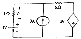
Determine the current in the 6 ohm resistor using Superposition Theorem
  1. 3.4 A
  2. 4.2 A
  3. 4.0 A
  4. 3.8 A
Superposition Theorem Solved Problems


Solution :

Note about this Exemple :


whene a source is operating alone, the other current sources must be opened while the other voltage sources must be short circuited

let the voltage source to operate alone.

Superposition voltage source

Apply KVL :

6+V1-I'(6) + 3V1=0
6+4V1 = 6I'1   Equation 1
V1I'=(I1= I'    Equation 2

substitute E.q.2 in E.q.1:

6 +4(I') = 6I'
I' = 6/2 = 3A
I' = 3A

Let the current source to operate alone.
Solution Superposition Theorem

Apply KCL at node 'a':

3 = I1 + I"
3 = V1/1+((V1 + 3V)/6)
3 = 1.667.V1

V1 = 1.8V

I"=(4V1/6) = ((4x1.8)/6 = 1.2 A

I = I' + I" =3 + 1.2

I = = 4.2 A

Note : Since the direction of currents of both I' and I" are the same, then the resultant current that will flow in the 6 ohm resistance, is equale to the arithmetic sum of the two currents respectively.


Friday, November 27, 2015

Millman's Theorem solved problems

Millman's Theorem explained

When any number of voltage sources of arbitrary generated voltage and finite Internal resistance different from zero are connected In parallel. the resulting voltage across the parallel combination is the ratio of the algebraic sum of the currents that each source individualy delivers when short circuited to the algebraic sum of the internal conductance.

Millman's equivalent circuit

millman's equivalent circuit

millman theorem formula

Exemple : solve I1 , I2 and I3

Milman Theorem solved problems

Step 1:

Draw the Millman's equivalent circuit and solve for Vab

millman's theorem equation

Step 2 : 

Solve for I1 , I2 and I3

Thursday, November 26, 2015

Thevenin's theorem principle

Thevenin's Theorem explained

If a resistor of R ohms be connected between any two terminals of a linear network, the resulting steady state current through the resistor is the ratio of the potential difference E0 ( V thevenin ) (between the two points prior to the connection ) and the sum of the values of resistance R0 ( R thevenin )  resistance between the two points. and the connected resistance R. Named after the french telegraph engineer, Charles Leon Thevenin (1857 - 1926).

Thevenin equivalent circuit

thevenin  equivalent circuit

Exemple : solve for I3:

thevenin theorem exercises

Solution :

Step 1 :


Open circuit R3 and solve for the voltage  across the open circuited terminals.
thevenin theorem solved problems

Note :

E0 is computed using any methods (kirchhoff's , maxwell , Nodal , etc .. ) of analysing network problems.

Step 2 :

compute R0 thevenin equivalent resistance or (short circuit all independant voltage sources and open circuits all independant current source ).
thevenin equivalent resistance

Note :

R0 is computed using the basic principles of finding the total resistance of a given circuit.

Step 3 :

construct the thevenin's equivalant circuit and solve the resulting current.

Thursday, November 19, 2015

Kirchhoff's law solved problems

kirchoff's law problems with solution

Kirchhoff law definition and principle

The sum of the currents flowing into a point in a circuit is equal to the sum of the currents flowing out of that same point.

In addition to providing the voltage law for series circuits, Gustav Kirchhoff (in 1847) was the first to observe and prove that the sum of all the branch currents in a parallel circuit (I1 + I2 + I3, etc.) was equal to the total current (IT). In honor of his second discovery, this phenomenon is known as Kirchhoff’s current law, which states that the sum of all the currents entering a junction is equal to the sum of all the currents leaving that same junction.
Figure 4-8(a) and (b) illustrate two examples of how this law applies. In both examples, the sum of the currents entering a junction is equal to the sum of the currents leaving that same junction. In Figure 4-8(a) the total current arrives at a junction X and splits to produce three branch currents, /1 I2, and I3, which cumulatively equal the total current (IT) that arrived at the junction X. The same three branch currents combine at junction Y, and the total current (Jr) leaving that junction is equal to the sum of the three branch currents arriving at junction Y Stated mathematically:

Kirchhoff law formula

IT = I1 + I2 + I3 + I4 ...


Problem law N°1

Refer to Figure 2 and calculate the value of IT.

Exercise Kirchhoff  law

Solution 1 :

By Kirchhoff’s current law,
IT = I1 + I2 + I3 + I4
IT = 2 mA + 17 mA + 7 mA + 37 mA

Problem  N°2

Refer to Figure 3 and calculate the value of IT

Kirchhoff s law exercises


Solution 2 :

By transposing Kirchhoff’s current law, we can determine the unknown value (IT):

IT = I1 + I2
7A = x + 3A
I1 = 4A

OR

IT = I1 +I2
IT - I2 = I1
I1 = IT - I2 = 7A - 3A =4A

DC current solved problems on serie resistor circuit

Solved Problems on serie circuit

Serie circuit definition

Circuit in which the components are connected end to end so that current has only one path to follow throughout the circuit.
Figure  illustrates five examples of series resistive circuits. In all five examples, you will notice that the resistors are connected “in-line” with one another so that the current through the first resistor must pass through the second resistor, and the current through the second resistor must pass through the third, and so on.
serie circuit definition

Problem  N°1

In Figure (a), seven resistors are laid out on a table top. Jsing a protoboard, coiinect all the resistors in series, starting at Rh and proceeding in numerical order through the resistors until reaching R7. After completing the circuit, connect the series circuit to a dc power supply.

solved exercise on serie circuit

Solution 1 :

in Figure (b), you can see that all the resistors are now connected in series (end-to-end), and the current has only one path to follow from negative to positive.
solved exercise on serie circuit

Problem serie circuit N°2

Figure (a) shows four 1.5 V cells and three lamps. Using wires, connect all of the cells in series to create a 6 V battery source. Then connect all of the three lamps in series with one another, and finally, connect the 6 V battery source across the three-series-connected-lamp load.
Exercise serie circuit N 2

Solution 2 :

In Figure (b) you can see the final circuit containing a source, made up of four series- connected 1.5 V cells, and a load, consisting of three series-connected lamps. As explained in Chapter 2, when cells are connected in series, the total voltage (Vr) will be equal to the sum of all the cell voltages:

VT=VX + V2 + V3 + V4 = 1.5 V + 1.5 V + 1.5 V + 1.5 V = 6 V

Tuesday, November 17, 2015

Full wave rectifier Problems

Problem 1 :  full wave rectifier

Calculate the average output voltage from a half-wave and full wave center tapped rectifier ifVipeak= 169.7 V.
Full wave rectifier Exercice

Solution problem 1

Full wave center tapped rectifier:

if Vs peak = 169.7 V, then Vs2 peak = 84.9 V

Vavg = 0.636 x (1/2) Vs peak
         = 0.636 x 84.9 = 54 V

Half-wave rectifier:

Vavg = 0.318 x Vs peak = 0.318 X 169.7 V = 54 V

As you can see from this example, even though the peak output of the full wave center tapped rectifier was half that of the half-wave rectifier, the average output was the same because the full wave center-tapped rectifier doubles the number of half-cycles at the output, compared to a half wave rectifier.

Problems 2 : Full & Half wave rectifier 

Calculate the average output voltage from a half-wave and full wave center tapped rectifier if K, peak = 169.7 V.

Solution problem 2

Half wave rectifier :

Vavg = 0.318 x Vs peak
         = 0.318 X 169.7 V = 54 V

Full wave center tapped rectifier:

If Vs peak = 169.7 V then Vs1 peak and Vs2 peak = 84.9 V

Vavg = 0.636 x (1/2) Vs peak
         = 0.636 x 84.9 V = 54 V

As you can see from this example, even though the peak output of the full wave center tapped rectifier was half that of the half wave rectifier, the average output was the same because the full wave center tapped rectifier doubles the number of half-cycles at the output, compared to a half-wave rectifier.

Problem 3 : Center-tapped rectifier

Calculate the average output voltage from a center tapped rectifier and a bridge rectifier if Vs peak = 169.7 V.

Solution problem 3

Center-tapped:

Vavg = 0.636 x (1/2) Vs

         =0.636 X 84.9 V
         = 54 V
Bridge:

Vavg = 0.636 X Vs
         = 0.636 X 169.7 V
         = 107.9 V

As you can see from this example, unlike the center-tapped rectifier that only connects half of the peak secondary voltage across the load, the bridge rectifier connects the total peak secondary voltage across the load.

Half wave rectifier Solved Problems

Problem 1

Calculate the following for the rectifier circuit shown in Figure
  1. Output polarity
  2. Peak and average output voltage, taking into account the diode’s barrier potential
  3. Output ripple frequency
Half wave rectifier exercise

Solution Problem 1

  1. Negative pulsating dc

  2. Vin peak = 169.7 V
    Vs = ( Ns / Np ) x Vp
          = ( 1/8 ) x 169.7 V peak = -21.2 V peak
    Vout = Vs - V diode
             =21.2 V - 0.7 V = -20.5 V
    Vavg = 0.318 x Vout
             = 0.318 x 0.5 V = -6.5 V

  3. Output ripple frequency = input frequency = 60 Hz


Half wave rectifier circuit Theory & Calculations

Half wave rectifier Definition

The half wave rectifier circuit is constructed simply by connecting a diode between the power supply transformer and the load, as shown in Figure (a). When the secondary ac voltage swings positive, as shown in Figure (b), the anode of the diode is made positive, causing the diode to turn ON and connect the positive half-cycle of the secondary ac voltage across the load (RL). When the secondary ac voltage swings negative, as shown in Figure (c), the anode of the diode is made negative, and therefore the diode will turn OFF. This will prevent any circuit current, and no voltage will be developed across the load (RL).

Half wave rectifier vutput voltage Formula

Figure (d) illustrates the input and output waveforms for the half wave rectifier circuit. The 120 V ac rms input, or 169.7 V ac peak input, is applied to the 17:1 step-down transformer, which produces an output of:
half wave rectifier output voltage formula

Because the diode will only connect the positive half-cycle of this ac input across the load (Rl), the output voltage (VRL) is a positive pulsating dc waveform of 10 V peak. In this final waveform in Figure (d), you can see that the circuit is called a half wave rectifier because only half of the input wave is connected across the output.
The average value of two half-cycles is equal to 0.637 V peak. Therefore, the average value of one half-cycle is equal to 0.318 V peak voltage of (0.637/2 = 0.318):

Vavg =0.318 x Vs peak

half wave rectifier circuit.
half wave rectifier basics
positive input half-cycle operation

In the example in Figure , the average voltage of the half-wave output will be:

                Vavg = 0.318 X Vs peak
          Vavg = 0.318 X 10 V
Vavg = 3.18 V

To be more accurate, there will, of course, be a small voltage drop across the diode due to its barrier voltage of 0.7 V for silicon and 0.3 V for germanium. The output from the circuit in Figure 1 would actually have a peak of 9.3 V (10 V - 0.7 V), and therefore an average of 2.96 V (0.318 X 9.3 V), as shown in Figure (e).
Vout =Vs - Vdiode 

Half wave rectifier Graph

half wave rectifier graph

Another point to consider is the reverse breakdown voltage of the junction or rectifier diode. When the input swings negative, as illustrated in Figure (c), the entire negative supply voltage will appear across the open or OFF diode. The maximum reverse breakdown voltage, or peak inverse voltage (PIV) rating of the rectifier diode, must therefore be larger than the peak of the ac voltage at the diode’s input.

Output Polarity of Half wave rectifier

Output polarity. The half wave rectifier circuit can be arranged to produce either a positive pulsating dc output, as shown in Figure (a), or a negative pulsating dc output, as shown in Figure (b). Studying the difference between these circuits you can see that in Figure (a) the rectifier diode circuit is connected to conduct the positive half-cycles of the ac input, while in Figure (b) the rectifier diode is reversed so that it will conduct the negative half-cycles of the ac input By changing the direction of the diode in this manner, the rectification can be made to produce either a positive or a negative dc output

half wave rectifier positive pulsating
 
half wave rectifier negative pulsating DC

Ripple frequency of Half wave Rectifier

Referring to the input/output waveforms of the half wave rectifier circuit shown in Figure 11-20, you can see that one output ripple is produced for every complete cycle of the ac input. Consequently, if a half wave rectifiers is driven by the 120 V ac 60 Hz line voltage, each complete cycle of the ac input and each complete cycle of the output will last for one-sixtieth or 16.67 ms (1/60 = 16.67 ms). The frequency of the pulsating dc output from a rectifier is called the ripple frequency, and for half wave rectifier circuits, the:
Ripple frequency of half wave rectifier

output pulsating DC ripple frequency = AC   frequency

Sunday, November 15, 2015

the Transient suppressor diode | Transorb

transient suppressor diode Definition

A device used to protect voltage-sensitive electronic devices in danger of destruction by high-energy voltage transients.

Transorb Definition

Absorb transients. Another name for transient suppressor diode.

Transient Suppressor Diode Uses


Lightning, power line faults, and the switching on and off of motors, air conditioners, and heaters can cause the normal 120 V rms ac line voltage at the wall outlet to contain under-voltage dips and over-voltage spikes. Although these transients only last for a few microseconds, the overvoltage spikes can cause the input line voltage to momentarily increase by 1000 V or more. In sensitive equipment, such as televisions and computers, shunt filtering devices are connected between the ac line input and the primary of the dc power supply’s transformer to eliminate these transients before they get into, and possibly damage, the system.

Transorb Schematic Symbol

Transorb Schematic Symbol

One such device that can be used to filter the ac line voltage is the transient suppresion diode. Referring to Figure (a), you can see that this diode contains two zener diodes that are connected back-to-back. The schematic symbol for this diode is shown in Figure (b).
Transient suppressor diodes are also called transorbs because they “absorb transients.” Figure (c) shows how a transorb would be connected across the ac power line input to a dc power supply. Because the zeners within the transient suppresion diode are connected back-to-back, they will operate in either direction (the device is “bi-directional”) and monitor both alternations of the AC input. If a voltage surge occurs that exceeds the Vz (zener voltage) of the diodes, they will break down and shunt the surge away from the power supply.

Transorb Circuit


Transorb Schematic Symbol

Most manufacturers’ transorbs have a high power dissipation rating because they may have to handle momentary power line surges in the hundreds of watts. For example, the Motorola 1N5908 1N6389 series of transorbs can dissipate 1.5 kW for a period of approximately 10 ms (most surges last for a few milliseconds). The devices must also have a fast turn-on time so that they can limit or clamp any voltage spikes. For example, the Motorola P6KE6.8 series has a response time of less than 1 ns.
In DC applications, a single unidirectional (one-direction) transient suppressor can be used instead of a bidirectional (two-direction) transient suppressor. These single transorbs have the same schematic symbol as a zener.

Metal Oxide Varistors MOVs


Transorb Schematic Symbol

Metal oxide varistors (MOVs) are currently replacing zener-diode and transient-diode suppressors because they are able to shunt a much higher current surge and are cheaper. These are not semiconductor devices in fact, they contain a zinc-oxide and bismuth-oxide compound in a ceramic body but are connected in the same way as a transient suppressor diode. They are called varistors because they operate as a “voltage dependent resistor” that will have a very low resistance at a certain breakdown voltage. The MOV’s schematic symbol, typical appearance, and construction are shown in Figure 2.

Saturday, November 14, 2015

Zener diode lesson

Definition of zener diode 


Zener Diode : is a Diodes constructed to operate at voltages that are equal to or greater than the reverse breakdown voltage rating.
Symbol of Zener diode

Zener diode principle


Figure 1(a) shows the two schematic symbols used to represent the zener diode. As you can see, the zener diode symbol resembles the basic P-N junction diode symbol in appearance; however, the zener diode symbol has a zig-zag bar instead of the straight bar. This zig-zag bar at the cathode terminal is included as a memory aid since it is “Z” shaped and will always remind us of zener.
Figure 1(b) shows two typical low-power zener diode packages, and one high- power zener diode package. The surface mount low-power zener package has two metal pads for direct mounting to the surface of a circuit board, while the axial lead low-power zener package has the zener mounted in a glass or epoxy case. The high-power zener package is generally stud mounted and contained in a metal case. These packages are.


identical to the basic P-N junction diode low-power and high-power packages. Once again, a band or stripe is used to identify the cathode end of the zener diode in the low- power packages, whereas the threaded terminal of a high-power package is generally always the cathode.

Characteristics voltage current 


Figure 2 shows the V-1 (voltage-current) characteristic curve of a typical zener diode. This characteristic curve is almost identical to the basic P-N junction diode’s characteristic curve. For example, when forward biased at or beyond 0.7 V, the zener diode will turn ON and be equivalent to a closed switch; whereas, when reverse biased, the zener diode will turn OFF and be equivalent to an open switch. The main difference, however, is that the zener diode has been specifically designed to operate in the reverse breakdown region of the curve. This is achieved, as can be seen in the inset in Figure 2, by making sure that the external bias voltage applied to a zener diode will not only reverse bias the zener diode (+ —» cathode, -  —» anode) but also be large enough to drive the zener diode into its reverse breakdown region.

As the reverse voltage across the zener diode is increased from the graph origin (which represents 0 volts), the value of reverse leakage current (Ir) begins to increase. Comparing the voltage developed across the zener (Vz) to the value of current through the zener (Iz), you may have noticed that the voltage drop across a zener diode (Vz) remains almost constant when it is operated in the reverse zener breakdown region, even though current through the zener (Iz) can vary considerably. This ability of the zener diode to maintain a relatively constant voltage regardless of variations in zener current is the key characteristic of the zener diode.

Generally, manufacturers rate zener diodes based on their zener voltage (Vz) rather than their breakdown voltage (VBr). A wide variety of zener diode voltage ratings are available ranging from 1.8 V to several hundred volts. For example, many of the frequently used low-voltage zener diodes have ratings of 3.3 V, 4.7 V, 5.1 V, 5.6 V, 6.2 V, and 9.1 V.

voltage current Characteristics

How to test zener diode with multimeter

Because a zener diode is designed to conduct in both directions, we cannot test it with the ohmmeter as we did the basic P-N junction diode. The best way to test a zener diode is to connect the voltmeter across the zener while it is in circuit and power is applied, as seen in Figure 3. If the voltage across the zener is at its specified voltage, then the zener is functioning properly. If the voltage across the zener is not at the nominal value, then the following checks should be made:

multimeter Test
  1. Check the source input voltage. If this voltage (Vin) does not exceed the zener voltage (Vz), the zener diode will not be at fault because the source voltage is not large enough to send the zener into its reverse breakdown region.
  2. Check the series resistor (Rs) to determine that it has not opened or shorted. An open series resistor will have all of the input voltage developed across it and there will be no voltage across the zener. A shorted series resistor will not provide any current-limiting capability and the zener could possibly bum out.
  3. Check that there is not a short across the load because this would show up as 0 V across the zener and make the zener look faulty. To isolate this problem, disconnect the load and see if the zener functions normally.
If these three tests check out okay, the zener diode is probably at fault and should be replaced.